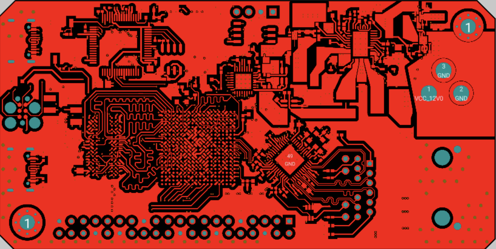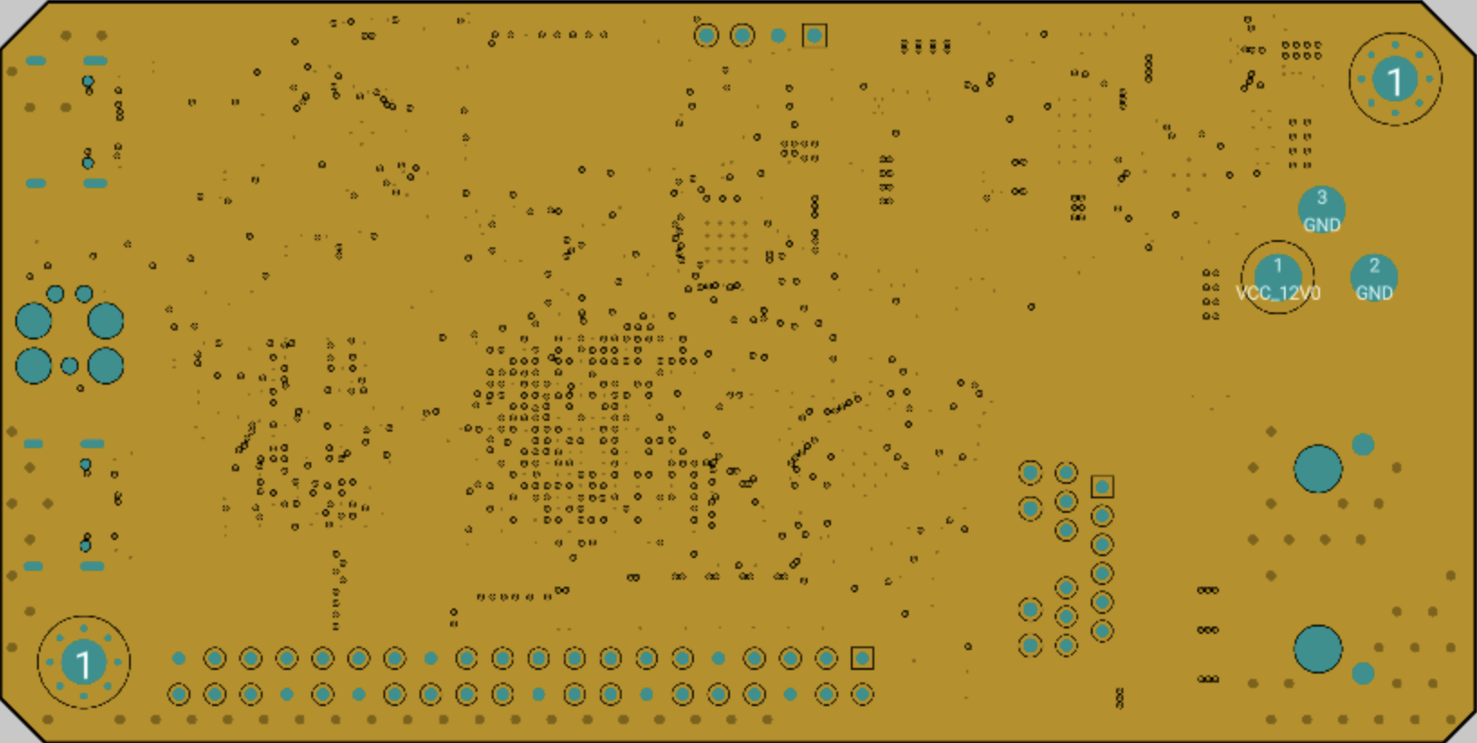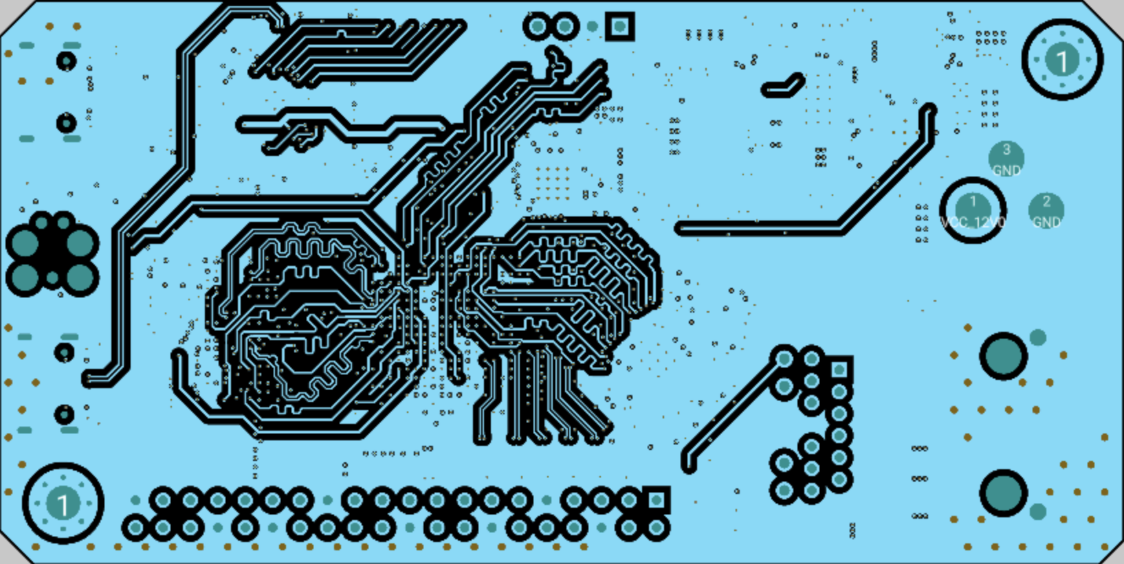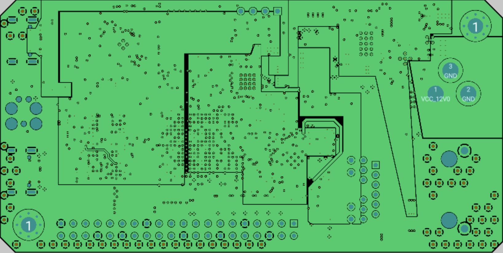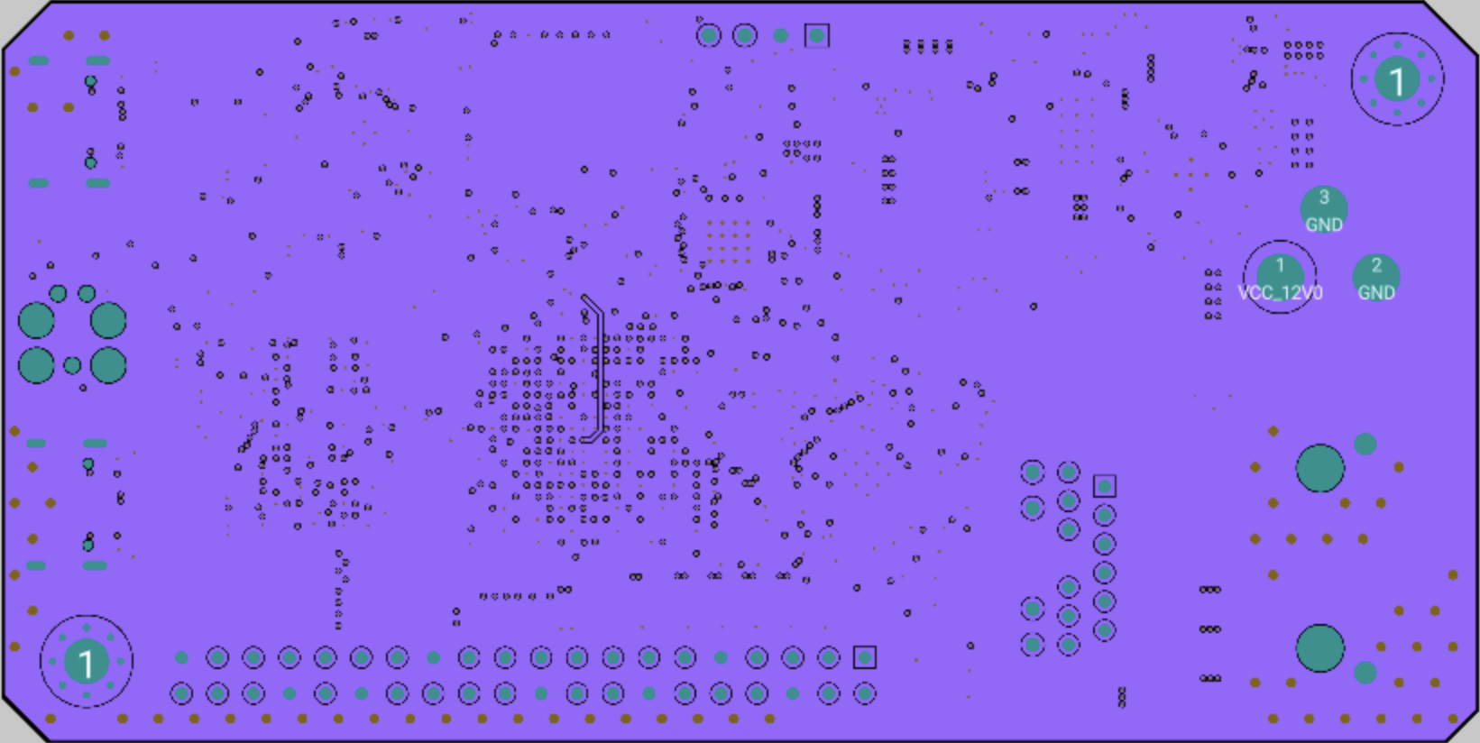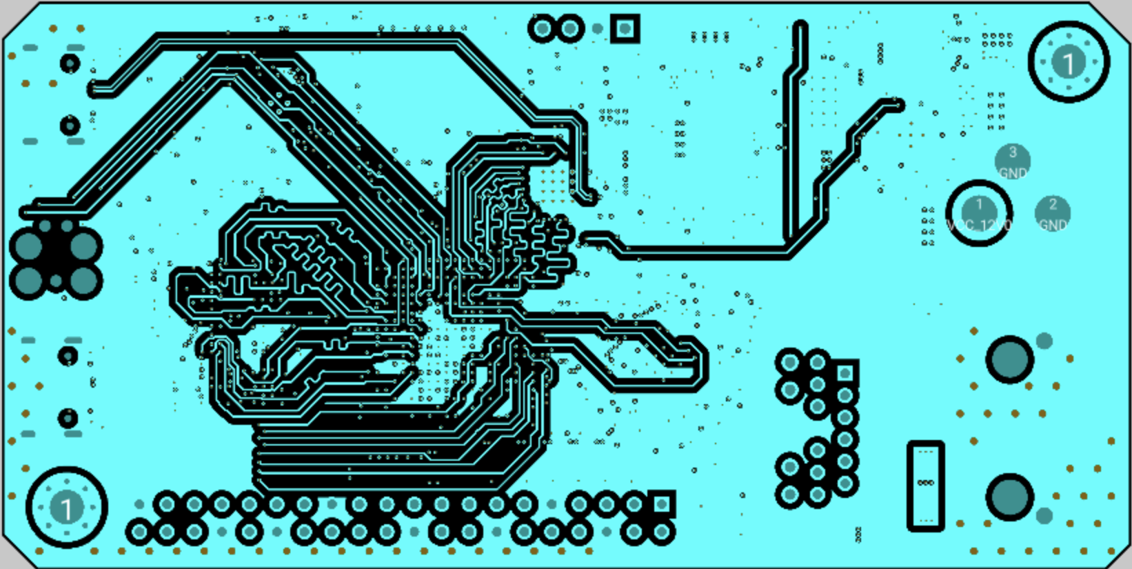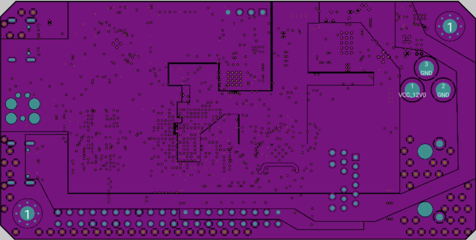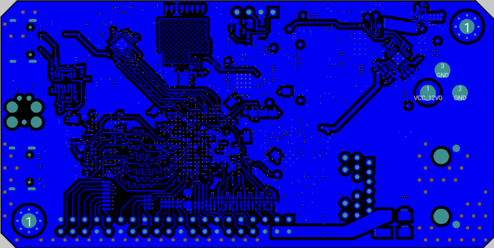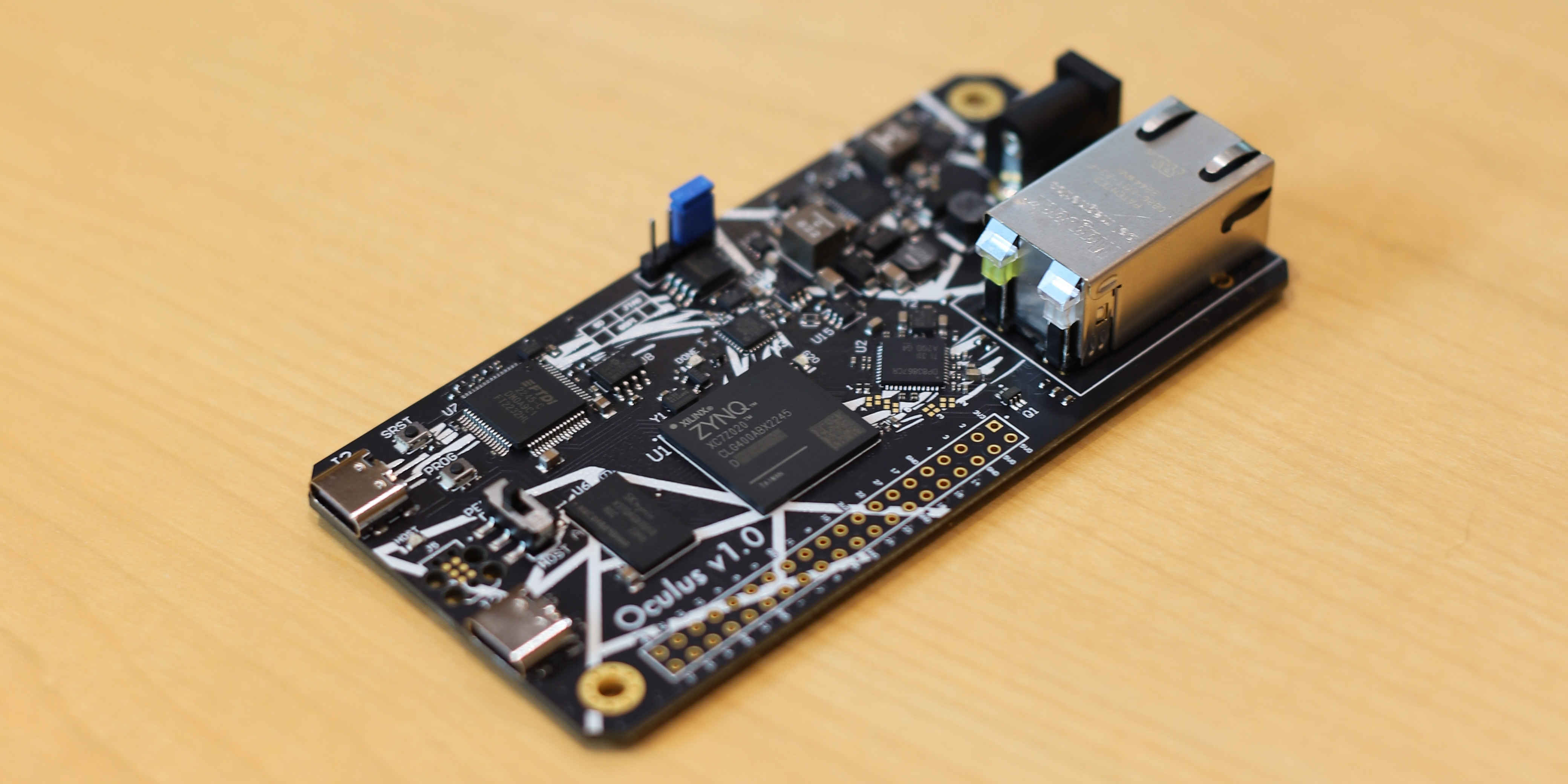
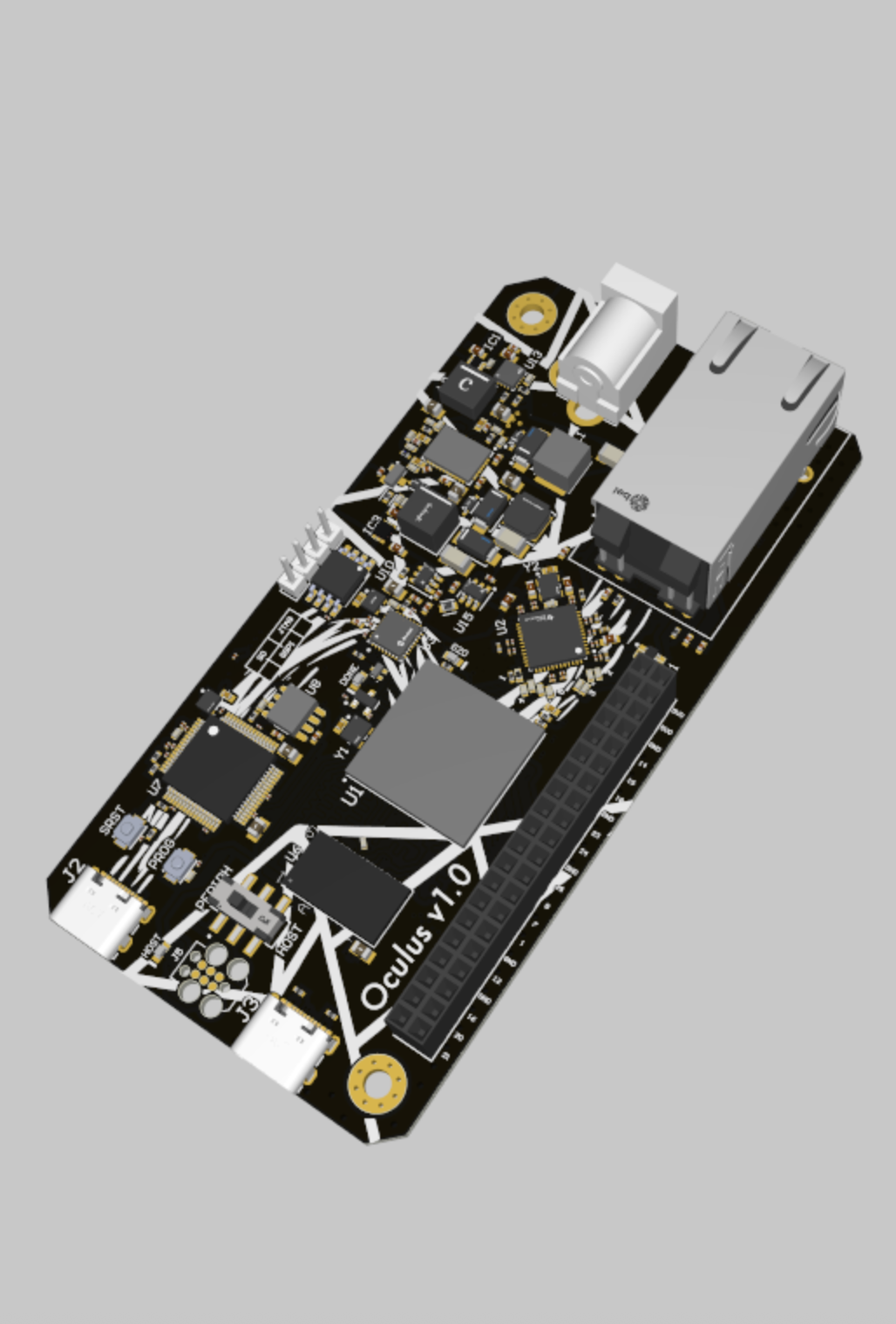
This is Oculus, an 8-layer FPGA accelerator board created in Altium intended to serve as a companion processor on the UAVs@Berkeley competition hexacopter. I did the schematic design and the majority of the layout for this board in the Spring 2025 offering of APE, a UC Berkeley Decal, while my partner worked on the firmware and RTL. One of UAVs@Berkeley's projects used the OpenCV implementation of ORB, a computer vision algorithm that is used to help match points in images together. Unfortunately, it runs at about 2 frames per second on our onboard computer, so I thought it would be an awesome experience to create a PCB to run a hardware implementation of it. Video data is streamed over RTSP into the ethernet port, processed on the FPGA, and output to the main onboard computer through USB 2.0. This particular form factor is compact and light, which is good for use aboard our drone where space and weight are at a premium.
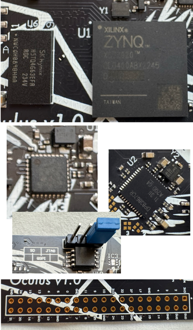
XC7Z020 400-BGA with two ARM cores and 85K PL cells for FPGA fabric. This was the cheapest FPGA that satisfied the requirements for the project, considering I was on a tight budget. This was also my first complex PCB design project, so I wanted something that had readily accessible example designs in case I couldn't figure something out on my own.
Intended to hold images while processing them in the FPGA. DDR3 is the fastest memory supported on this FPGA, and I was fine with an extra voltage level on the board.
DP83867CR ethernet PHY for RTSP video stream input. The camera on the UAVs@Berkeley competition hexacopter sends video data as an RTSP stream, so this was needed. It also opens the board up to more applications for use as a development tool. This particular PHY was chosen because of its clear documentation and availability.
USB3320 USB 2.0 PHY with user-selectable host/peripheral mode. This is the fastest USB data protocol the FPGA supports, and it has pretty solid data transfer rates (480Mbps). That is more than enough to transfer low-resolution images and key point information to the onboard computer.
JTAG, QSPI, and SD card for large boot images.
GPIO pins connected to FPGA fabric to expand functionality of the board.
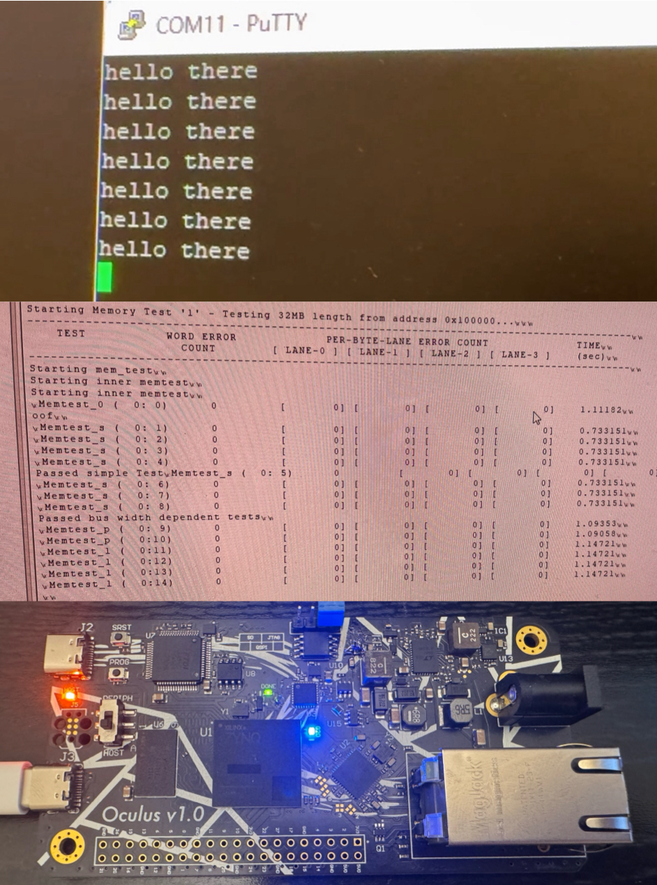
This was a huge yet very rewarding project for me, and I am very proud that the board powered on and was able to be programmed! In the past, I have only designed two-layer boards in KiCAD, so making the jump all the way to 8 layers in Altium was a bit daunting at first. If I were to redesign the board, I would make several changes. First off, the DDR3 layout can definitely be optimized to potentially fit on 6 layers. To minimize the footprint of the board, I would remove the FTDI chip and spare USB port, and move more components to the back of the board. I would also completely rework the voltage levels with a programmable converter, which would make setting power up and power down sequences significantly easier.